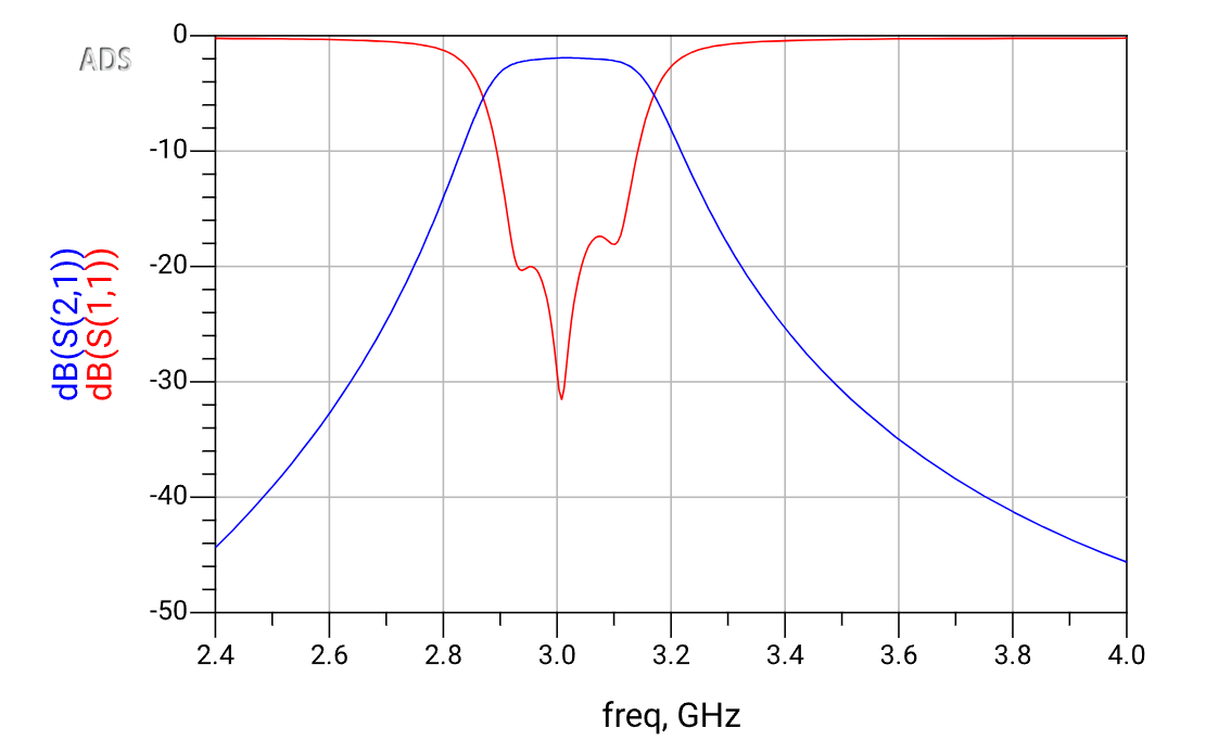
ADS / EM simulation. Passband centered close to 3 GHz with roughly 3 dB insertion loss and good matching near the center frequency.
Analytical design, ADS optimization, PCB implementation and VNA measurement.
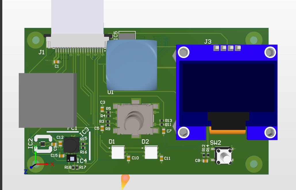
The 3 GHz coupled-line band-pass filter was developed from analytical calculation through simulation and physical measurement. Even- and odd-mode quantities were calculated in MATLAB, followed by implementation in Keysight ADS. The filter was then tuned and optimized before fabrication and VNA characterization.
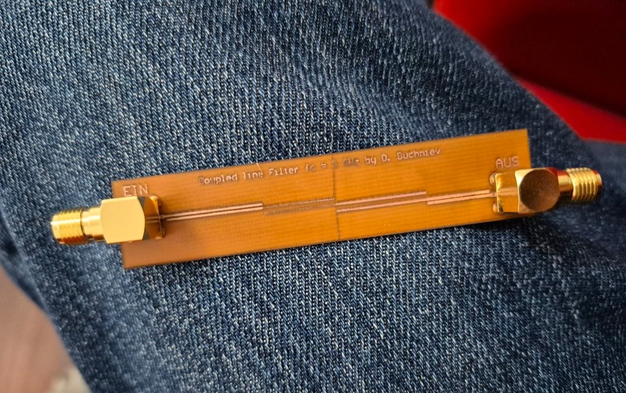
The prototype PCB was fabricated using an LPKF PCB prototyping system. Compared with an industrial multilayer RF PCB process, mechanical prototyping introduces additional practical loss mechanisms such as conductor-surface quality, milling accuracy, transition geometry and connector/soldering imperfections.
ADS / EM simulation. Passband centered close to 3 GHz with roughly 3 dB insertion loss and good matching near the center frequency.
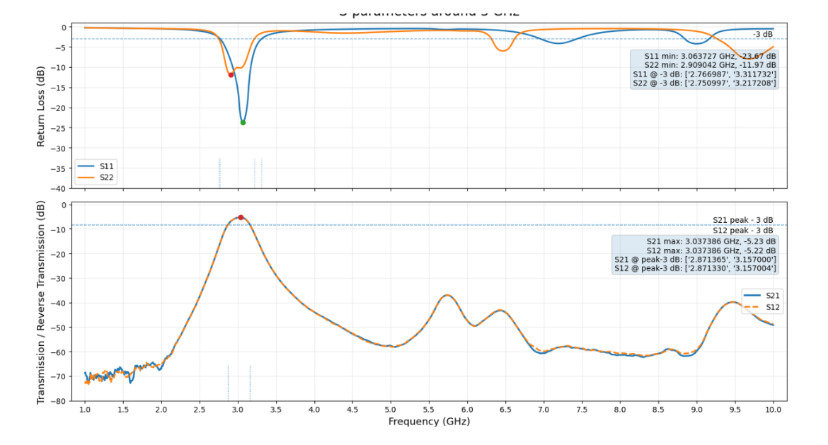
Measured S-parameters. Transmission peaks at about −5 dB near 3.04 GHz, with S11 reaching about −23.7 dB in the passband.
The EM model predicts about 3 dB insertion loss, while the fabricated filter measures about 5 dB. The difference is mainly explained by real PCB losses and tolerances: FR-4 dielectric loss and material variation, copper loss and surface roughness, SMA launches and solder joints, plus small fabrication errors that affect coupling in the narrowband structure.